Getting Started with the KITPF5030FRDMEVM Evaluation Board
Contents of this document
-
Out of the Box
-
Get Hardware
-
Get Software
-
Configure Hardware
Sign in to save your progress. Don't have an account? Create one.

Purchase your KITPF5030FRDMEVM
1. Out of the Box
The NXP analog product development boards provide an easy-to-use platform for evaluating NXP products. The boards support a range of analog, mixed-signal and power solutions. They incorporate monolithic integrated circuits and system-in-package devices that use proven high-volume technology. NXP products offer longer battery life, a smaller form factor, reduced component counts, lower cost and improved performance in powering state-of-the-art systems.
This page will guide you through the process of setting up and using the KITPF5030FRDMEVM board.
1.1 Kit Contents and Packing List
The KITPF5030FRDMEVM kit contents include:
1.2 Additional Hardware
In addition to the kit contents, the following hardware is necessary or beneficial when working with this kit.
- One or two power supplies with a range from 3.3 V to 5.0 V and a current limit set initially to 1.0 A
1.3 Windows PC Workstation
This evaluation board requires a Windows PC workstation. Meeting these minimum specifications should produce great results when working with this evaluation board:
- USB-enabled computer with Windows 7 or Windows 10
2. Get Hardware
2.1 Board Features
- VIN power supply connector (1x or 2x 3.3 V to 5.0 V)
- BUCK1 and BUCK2: 0.7 V to 1.5 V up to 1.0 A (socket limit)
- BUCK3: 1.0 V to 3.3 V up to 1.0 A (socket limit)
- LDO1 and LDO2: 1.5 V to 5.0 V
- PWRON switch
- FS0B external safety pin
- Embedded USB connection for easy connection to software NXP GUI (access to I²C bus, IOs, RSTB, FS0B, INTB, debug, AMUX_OUT, regulators, register access, OTP emulation and OTP programming)
- LEDs that indicate signals and regulator status
- Support OTP fuse capabilities
- Voltage monitoring jumper setting
2.2 Board Description
The KITPF5030FRDMEVM is a hardware evaluation tool that allows OTP burning. Due to the socket, PF5030 part can be configured without the need to solder it. Devices can be programmed two times.
The KITPF5030FRDMEVM is a hardware evaluation tool that allows performance test. PF5030 can be evaluated with this board because it is populated with a superset part. The PPF5030BMDA0ES part soldered on the board can be fused twice.
2.3 Board Components
Overview of the KITPF5030FRDMEVM board

| Number | Description |
|---|---|
| 1 | VIN_5V and VIN_3V3 power supply input |
| 3 | VIN three position switch
|
| 4 | BUCK1/2 regulators output |
| 5 | BUCK3 regulator output |
| 6 | LDO1/2 regulators output |
| 7 | USB connectors (OpenSDA for MCU flash; KL25Z for NXP GUI control) |
| 8 | Debug connectivity. Access to PF5030 signals |
| 9 | PWRON switch |
| 10 | VMON_EXT resistor bridge configuration (choice between monitoring 3.3 V or 5.0 V) |
| 11 | OTP mode switch |
| 12 | DBG pin to ground if unplugged |
| 13 | BUCK1 inductor current measurement jumper |
| 14 | BUCK2 inductor current measurement jumper |
| 15 | BUCK3 inductor current measurement jumper |
| 16 | KL25Z FRDM board connectors |
| 17 | VLED supply configuration |
3. Get Software
3.1 Install and Configure Software and Tools
The programming/evaluation boards are always delivered with the GUI firmware already flashed. If MCU firmware already flashed, you can ignore this section. If it is specified that firmware must be updated or it is malfunctioning, follow these instructions.
3.2 Flash or Update the FRDM-KL25Z GUI Firmware
If bootloader is already loaded in the FRDM-KL25Z board, steps 1-3 are not required. Start from step 4.
-
Disable the Storage Service and Windows Search: Run Services, double click, and stop them as shown in Figure 1.

-
Press the RST push button and connect the USB cable to the SDA port on the FRDM-KL25Z board
- A new “bootloader” device appears on the left pane of the file explorer
- Drag and drop the file “MSD-DEBUG-FRDM-KL25Z_Pemicro_v118.SDA” to the bootloader drive Ensure that there is enough time for the firmware to be saved in the bootloader
-
Disconnect the USB cable, then reconnect it to the SDA port WITHOUT pressing the RST push button
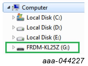
- This time, FRDM_KL25Z device appears on the left pane of the file explorer as in Figure 2
- Locate the file
nxp-gui-fw-frdmkl25z-usb_hid-device.binfrom the package. Drag and drop this file into the FRDM_KL25Z device Ensure that there is enough time for the firmware to be saved. - FRDM board firmware is successfully loaded. Disconnect the USB-cable and reconnect it to the KL25Z USB port.
3.3 Install NXP GUI Software Package
To install the "NXP GUI for Automotive PMIC Families" or obtain the NXP GUI package, unzip an open "1 - NXP_GUI_Setup" folder as shown in Figure 3.

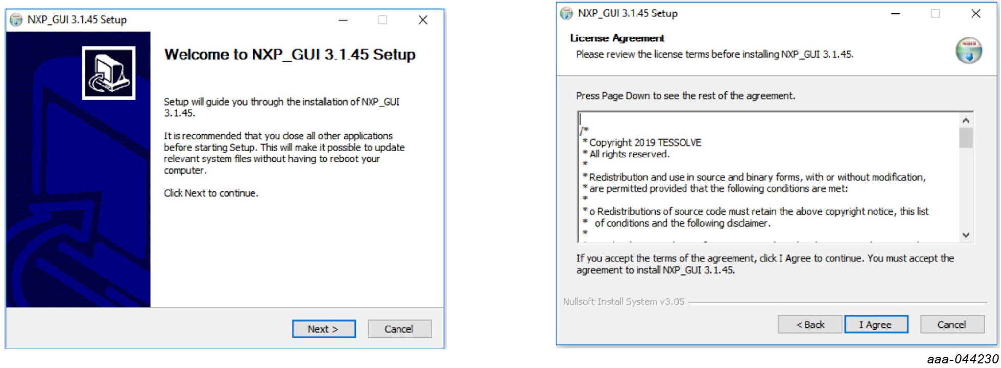
Then double click on the "NXP_GUI-version-Setup.exe" shown in Figure 4 and follow the instructions.

To install the application on Windows PC, proceed with the pop-up windows shown in Figure 5 and Figure 6.
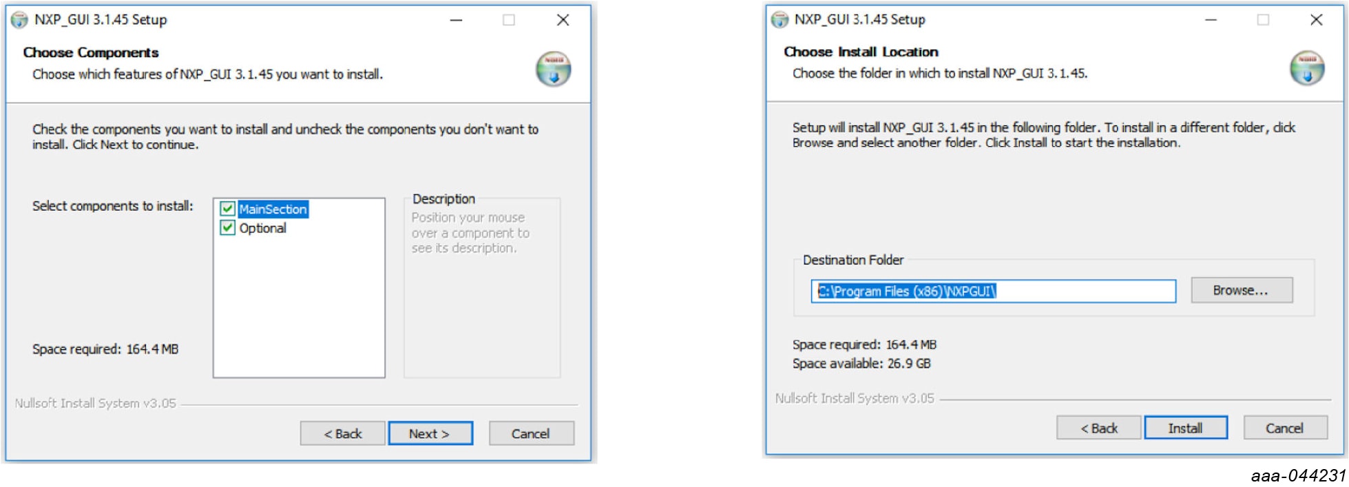
Select the options shown in Figure 7 before completing the installation of the setup:
- Run NXP_GUI
- Show Readme
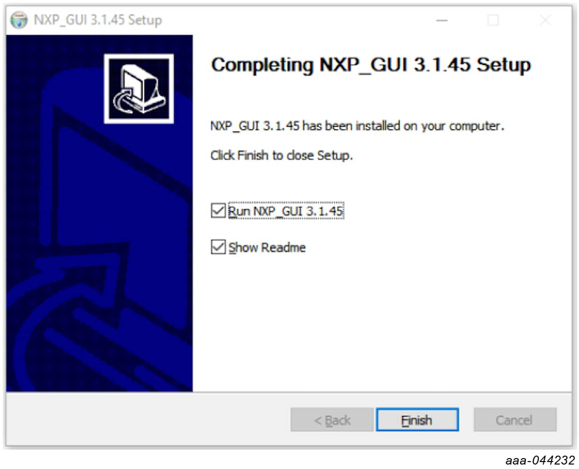
Select Finish to complete the installation.
When installation is finished, you can search the application on the Windows search bar as “NXPGUI”. Click to launch.
4. Configure Hardware
4.1 Configure the Hardware
Figure 8 presents a typical hardware configuration incorporating the development board, power supply and, Windows PC workstation.

To configure the hardware and workstation, complete the following procedure:
- Install jumpers and switches for the configuration shown in Table 2.
- Connect the Windows PC USB port to the KITPF5030FRDMEVM board using the provided USB 2.0 cable.
- If external power supplies are used, set the power supplies to 3.3 V and 5.0 V and current limit to 1.0 A. With power turned off, attach the power supplies positive and negative outputs to J1, then turn on.
- Put
SW5in LEFT position if USB power is used or RIGHT position if external power supply is used.
| Board Configuration | Configuration | ||
|---|---|---|---|
| Normal mode | Debug mode entry | OTP / test mode entry | |
| Watchdog configuration | Watchdog windowing enabled, 2 seconds INIT_FS timeout (OTP WDW_INF = 0) | Watchdog windowing disabled, no INIT_FS timeout | OTP programming / emulation, Debug mode enabled |
| Watchdog windowing disabled, no INIT_FS timeout (OTP WDW_INF = 1) | |||
J3 (DBG) |
Open | Connect 1 to 2 DBG pin voltage pulled to 4.5 V or 7.95 V ( SW1) |
|
SW2 (PWRON) |
Close (PWRON pin high-logic level) | ||
SW5 (VIN) |
Middle position (supplies OFF) | ||
SW1 (OTP mode) |
Open (DBG = VIN_5V) | Close (OTP mode ON) | |
At this step, if the product is in OTP mode entry configuration, all regulators are OFF. The user can power up with an OTP configuration or configure the mirror registers before powering up. Power-up sequence starts as soon as one of these four actions occurs:
J3jumper is removedSW1is switched OFF- OTP mode exit command is sent using I²C
- NXP GUI button "Exit OTP Mode" is clicked
Design Resources
Additional References
In addition to our PF5030, Multi-Channel PMIC for Automotive Applications page, you may also want to visit: