- Smarter World Blog
- Designing a 5G mmWave Antenna Means Balancing Tradeoffs
Designing a 5G mmWave Antenna Means Balancing Tradeoffs

The 5G new radio frequency range 2 (NR FR2) spectrum above 24 GHz, known as millimeter Wave (mmWave), offers exceptionally high throughput speeds and is capable of supporting an enormous number of devices, but the signals in this range are very different from those found at or below 6 GHz, where most cellular developers are used to working.
Building an active phased-array antenna for 5G mmWave requires a very compact design. The antenna elements need to be placed at a distance of half wavelength, which is 5 mm. At the same time, each antenna element needs to have a transmit/receive channel connected to two polarization feeds. There is the corporate network to include, too, and the entire design has to deliver high heat flux in a small area. Creating a stacked PCB that meets all these requirements is a challenge, even for the most experienced engineers.
Small variations in operating parameters can cause the antenna to behave unexpectedly, leading to redesigns, reproduction and retesting of components, subsystems and even the entire system, resulting in a longer development cycle and higher development cost. There are physical conditions to consider, too, since production, assembly and day-to-day operating conditions can expose delicate electronic components to crushing pressure and damaging fluctuations in heat and temperature. Add to these challenges the fact that most design teams are working to meet tight deadlines and hit strict delivery dates, and the learning curve for anyone new to 5G mmWave technology can feel especially steep.
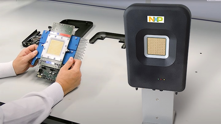
We say all this with first-hand experience, because our team just completed development of a 64-element antenna demonstrator that operates in the 5G mmWave range of 24 GHz to 28 GHz.
Projects like these, where we, as a semiconductor company, produce a system-level design, help us to help our customers. Working at the system level gives us the in-house expertise to guide our customers as they address various design challenges and, perhaps more importantly, creates a production-ready solution that lets our customers skip large portions of the learning curve. In other words, we go through the entire development process – making tradeoffs, evaluating choices and refining our designs – so our customers don’t have to.
Our Story
The image below shows an exploded view of what the NXP team has created.

To design the antenna, calibrate it and measure its performance required a team of more than two dozen subject-matter experts, working at NXP and at key partners for manufacturing and antenna design, and drew on their knowledge in such varied disciplines as beam-pattern validation, thermodynamics, AC/DC and DC/DC converter design, LVDS control, FPGA design and PCB manufacturing.
The Core Component
At the heart of most 5G mmWave antenna designs is the beamforming IC, which focuses high-frequency signals toward a specific receiver, making a connection that is more direct, faster, of higher quality and more reliable. Multiple beamforming ICs are connected and arranged in a regular structure, called a phased array. The phased array combines signals to produce radiation patterns that aren’t possible with individual antennas. Beamforming is used to vary the amplitude and phase of each antenna element’s signal, making it easier to focus and steer the beams.
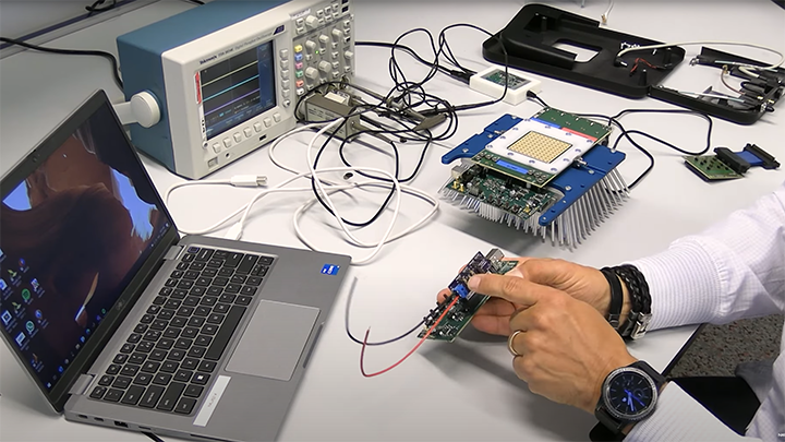
Our 64-element antenna demonstrator design helps developers save time and effort. Watch the getting started process and tips for obtaining calibration measurements.
The best beamformer IC helps optimize the overall performance, power consumption and cost of each radio element, so it’s a natural place to start when considering design options. In our case, we used the NXP MMW9014 beamforming IC, a highly integrated 5G 4-channel dual-polarized analog beamforming IC, housed in a very small FO-WLPBGA package (6.5 mm x 6.1 mm x 0.56 mm) with 182 bumps.
Having chosen a beamformer, the next step was to build the antenna panel PCB and the housing. This proved to be particularly important – and particularly tricky.

Preventing Warpage
One of the biggest challenges we faced was the trade-off between antenna warpage and heat management. We needed to achieve the right electromagnetic (EM) performance to create an antenna that would reliably operate at the desired frequency, while ensuring a stable thermal environment that protected the electronics from malfunctioning and kept the Antenna PCB from warping.
We were aiming for a warpage target of less than 0.22%, but exceeded this with ratings that measure between just 0.132% and 0.175%. The very low warpage rating is the result of several important design decisions. Having designed our antenna element, we mapped that structure to the requirements we had for the antenna, control, corporate network, supply lines and ground structure. This resulted in a 12-layer PCB built up symmetrically around a central core. Any warpage is the result of accumulated stress, due to the different thermal properties of the PCB’s metal and dielectric elements.
As shown in the diagram, the bottom six layers of the PCB create the antenna, and the top six layers manage the feed, supply, and analog and digital distribution.

The PCB stack is symmetrical on the z-axis. Knowing that the presence of copper would interfere with the operation of the antenna elements, we distributed all the system’s copper around the sides of the PCB, away from the antenna array.
To further improve the antenna’s reliability, and make the PCB more resilient against failures due to thermal cycling, we limited the number of stacked vias to three, and used staggering if higher via counts were needed. Staggered vias offset the damaging effects of having different thermal-expansion coefficients on different PCB materials, such as copper and dielectric. High temperatures occur at the manufacturing stage – especially when soldering takes place – and this approach reduces warpage even after soldering.
To prevent the heat sink from damaging the small, delicate MMW9014K package, we kept the clamp force to less than 1 gram per ball, and thereby prevented shorting due to solder-ball creep over the antenna’s operating life.
As an added protection for the PCB, and to help maintain its shape, we placed the PCB in an adjustable frame. Built of nylon on one side, for minimum antenna interference, and metal on the other, the adjustable frame lets us mount the PCB without adding to the physical stress placed on delicate circuitry.

Keeping Cool
We needed to manage the heat flow in order to guarantee the lifetime of the IC. This was another reason to minimize warpage, because it meant we could use a very thin thermal-interface material (TIM). The TIM is often the item with the highest thermal resistance within the thermal chain, so the goal is to keep it as thin as possible. To simplify assembly, the TIM is applied globally over the heatsink interposer, which is the anchor for the demonstrator’s mechanical design. The demonstrator’s physical casing is removable, so all the internal connectors are easy to access. We found this very helpful when working in smaller, space-constrained antenna-measurement rooms.
The mmWave splitting network is implemented as a corporate splitter. To improve isolation between the splitter and the antenna feeds, we placed transmission lines on an inner layer. The result is oscillation-free behavior, even with the beamformer’s 30 dB of gain. We also designed the transmission lines to work with the TIM and the heatsink, to support the design’s thermal requirements. The antenna’s scan range is ±45°.
Lastly, the decisions we made for Vcc distribution simplify the design and make it more efficient. We use a 19V supply to generate the necessary 2.8V for operation, making it possible to use a single supply from a standard AC/DC converter and reducing the amount of cabling needed in the antenna-measurement room. The current paths for all supply lines are designed to have both the forward and the return paths in designated places.
Ready to Run
Using our project team’s combined expertise, and leveraging NXP’s long history of success with antenna arrays and high-volume manufacturing, we created a standalone solution for use by anyone building a 5G mmWave antenna array.
The panel demonstrator is shipped in a kit that includes everything needed to analyze antenna parameters, including the temperature of each antenna in the array. The demonstrator is fully calibrated for antenna patterns, validated for beam patterns and follows manufacturing guidelines for high volume, so design teams can quickly go from prototype to mass manufacturing with a system that uses tight design rules for things like trace width, blind vias and layer thickness.
A separate evaluation kit, supplied with an AC/DC converter and example code in .dll format, for use with Matlab, provides additional options for analysis. The demonstrator is also available with an FPGA interface board that converts the USB connection from a PC to the LVDS master and control signals used by the antenna array.

We wish to thank the whole team who contributed to the project:
NXP: Mustafa Acar, Konstantinos Giannakidis, Harm Voss, Nick Spence, Arthur van de Kerkhof, Ashutosh Dwivedi, Dick van de Broeke, Evert van Capelleveen, Jan Willem Bergman, Jeroen Zaal, Arjan van den Berg, John Janssen, Rajesh Mandamparambil, Ramon Groot Wesseldijk and Paul Mattheijssen.
TNO: Roland Bolt, Erwin Suijker and Stefania Monni.
Philips: Yizhe Yin, Arthur van Es, Ruud Olieslagers, Nico van Dijk, Peter Snoeijen, Randy Kesselmans, Bas Driessen and Erik van Weert.
LV Electronics: Carlos Verdonck
TU/e and AntenneX: Teun van den Biggelaar and Roel Budé
Authors

Marcel Geurts
Marcel Geurts is Principal System Architect and Customer Program Manager. In this role, he focuses on NXP’s Radio Products’ mmwave, pre-driver and RxFEM portfolio for customer support and cooperation programs. He was responsible for the 26 GHz Antenna Panel Demonstrator design, validation and is supporting the customers in the usage of it.

Johan Janssen
Johan Janssen is Principal Application engineer. In this role, he focuses on NXP’s RF products intended for the infrastructure, and supports customers in applying products as LNA’s, ABF’s, RXFEMs in their final system. He was involved in the 26 GHz Antenna Panel Demonstrator design, validation and is supporting the customers in the usage of it.

