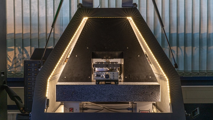
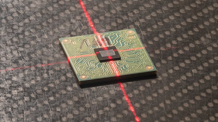
Product Analysis Flow
-
Step 1 - Reproduce the Failure in a Lab Environment
Our product analysts use evaluation boards, digital testers and other tools to replicate the customer issue in our labs.

-
Step 2 - Package Analysis
We first determine whether there is a physical defect with the IC package that surrounds the die.

-
Step 3 - Defect Spatial Localization
If there is no defect in the package, we remove the device package to expose the silicon die and use localization techniques to narrow down the subset of transistors that may have a defect.

-
Step 4 - Electrical Analysis
Once the problem area has been found, advanced analysis techniques are used to pinpoint the individual transistor or component that may be causing the observed failure mode.

-
Step 5 - Physical Analysis
We identify the physical, spatial, and material characteristics of the defect that correlates to the electrical signature of the failing component.

-
Step 6 - Documenting the Analysis
Results from the analysis are documented and made available to the necessary teams for corrective actions.

