Getting Started with the KITFS26SKTEVM Evaluation Board
Contents of this document
-
Get Started
-
Get the Hardware
-
Install Software
-
Configure the Hardware
Sign in to save your progress. Don't have an account? Create one.

Purchase your KITFS26SKTEVM | FS26 Safety SBC Programming Socket Board
1. Get Started
The NXP analog product development boards provide an easy-to-use platform for evaluating NXP products. The boards support a range of analog, mixed-signal and power solutions. They incorporate monolithic integrated circuits and system-in-package devices that use proven high-volume technology. NXP products offer longer battery life, a smaller form factor, reduced component counts, lower cost, and improved performance in powering state-of-the-art systems.
This page will guide you through the process of setting up and using the KITFS26SKTEVM evaluation board.
1.1 Kit Contents/Packing List
The KITFS26SKTEVM contents include:
- Assembled and tested evaluation board and preprogrammed FRDM-KL25Z microcontroller board in an anti-static bag
- 3.0 ft USB-STD A to USB-B-mini cable
- Two connectors, terminal block plug, 2 pos., str. 3.81 mm
- Three connectors, terminal block plug, 3 pos., str. 3.81 mm
- Jumpers mounted on board
- Quick start guide
1.2 Additional Hardware
In addition to the kit contents, the following hardware is necessary or beneficial when working with this kit.
- Power supply with a range of 8.0 V to 40 V and a current limit set initially to 1.0 A
2. Get to Know the Hardware
2.1 Board Features
- VBAT power supply connectors (Jack and Phoenix)
- LQFP48 burn in open top socket
- VPRE output output voltage from 3.2 V to 6.35 V, current capability up to 1.5 A
- VBOOST in independent mode or in front-end topology to support battery cranking profiles
- VCORE output voltage from 0.8 V to 3.35 V, current capability up to 1.65 A
- LDO1 and LDO2 from 3.3 V or 5.0 V, up to 400 mA
- VTRK1 and VTRK2, from 3.3 V or 5.0 V, up to 150 mA
- VREF 0.75 % accuracy regulator for external ADC reference
- FS0B, FS1b external safety pins
- USB to SPI protocol for easy connection to software GUI
- LEDs that indicate signal or regulator status
- Manual or Automated OTP fuse programming
- Advance system monitoring via AMUX or external ADC
- Analog variable resistor to test external VMON
2.2 Board Description
The KITFS26SKTEVM provides flexibility to play with all the features of the device and make measurements on the main part of the application. The KL25Z FRDM connected to the board, combined with the FS26 NXP GUI software allows to fully configure and control FS26 SBC. The LQFP48 Socket on board allows to test or to program different samples.
An FS26 SBC sample must be inserted in the socket to enable OTP programming, emulation or evaluation. The performance on this board is limited and KITFS26AEEVM must be used for further evaluation.
2.3 Board Components
Overview of the evaluation board

- VBAT Phoenix connector
- VBAT3 position switch
- VBAT Jack connector
- VDDIO selection
- Regulators outputs
- WAKE1 and WAKE2 inputs switches
- LQFP48 socket
- KL25Z FRDM headers (bottom)
- VDEBUG pin source selection (switch or MCU)
- VDEBUG pin voltage level switches
- VDDIO USB voltage level selection
- VMONEXT variable resistor
- Signal connector
- Program connector
- Regulators output LED indicators
- Program burning voltage LED indicator
- Safety output LED indicators
- Debug mode LED indicator
3. Install Software
The programming/evaluation boards are always delivered with the GUI firmware already flashed. If the MCU firmware is already flashed, this section can be ignored. If it is specified that the firmware must be updated, or if it is malfunctioning, follow these instructions.
3.1 Flashing or Updating the GUI Firmware
The KITFS26SKTEVM is delivered with the GUI firmware flashed. If MCU firmware is flashed, ignore this section. If it is specified to update the firmware or it is malfunctioning, follow the instructions below.
3.2 Flashing FRDM Board Firmware from Windows 7/10
If BOOTLOADER is already loaded in the FRDM Board, steps 1 to 3 are not required. Start from step 4.
-
Disable the Storage Service and Windows Search: Run Services, double click, and stop them as shown below
 Steps 2 and 3 are not required if BOOTLOADER is already loaded in the FRDM board
-
Press the RST push-button and connect the USB cable into the SDA port on the FRDM board.
A new “BOOTLOADER” device should appear on the left pane of the File explorer. -
Drag and drop the file “MSD-DEBUG-FRDM-KL25Z_Pemicro_v118.SDA” to the BOOTLOADER drive.
-
Disconnect and reconnect the USB cable into the SDA port.
This time without pressing the RST push-button, FRDM_KL25Z device should appear on the left pane of the File explorer as pictured below.
-
Locate the file “nxp-gui-fw-frdmkl25z-usb_hid-fs2630_vX.Y.bin” from the package and drag and drop the file into the FRDM_KL25Z device.
- FRDM board Firmware is successfully loaded. Disconnect and reconnect the USB cable into the KL25Z USB port.
3.3 Installing GUI Software Package
To install the FS26 NXP GUI, download or obtain the NXP GUI package, unzip 1- NXP_GUI_Setup folder:

Then, double-click NXP_GUI_version-Setup.exe and follow the instructions.

To install the application on Windows PC, proceed with the following pop-up windows:

Figure 1. Application Setup

Figure 2.License Agreement

Figure 3.Select FS2630_GUI

Figure 4. Choose the folder to install
Select the following options before completing the installation of the setup:
- Run NXP_GUI
- Show Readme
Select Finish to complete the installation.

Figure 5. Run NXP_GUI
When the installation is finished, you can find the application by searching for NXPGUI in the windows search bar. Click to launch.
4. Configure the Hardware
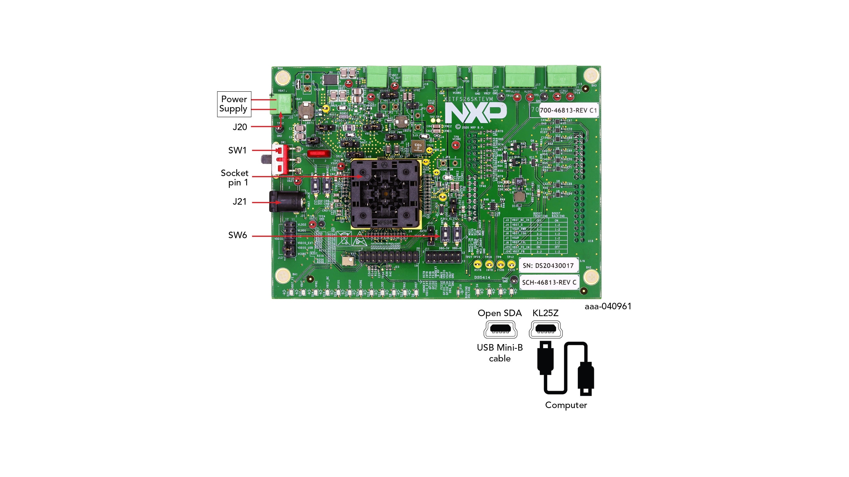
Figure 6. Typical initial configuration
To configure the hardware and workstation, complete the following procedure:
- With SW1 in middle position, set DC power supply to 12 V and current limit to 1.0 A. Attach the DC power supply positive and negative output to KITFS26SKTEVM VBAT Phoenix connector (
J20). Or connect 12 V power supply to VBAT Jack (J21)
4.1 VBAT Phoenix connector (J1)
| Schematic label | Signal name | Description |
|---|---|---|
| J20-1 | VBAT | Battery voltage supply input |
| J20-2 | GND | Ground |
4.2 VBAT Three Position Connector (SW1)
| Schematic label | Signal name | Description |
|---|---|---|
| SW1 pin 2-3 | VBAT Phoenix | Board supplied by Phoenix connector |
| SW1 pin 2 (middle position) | VBAT | Board not supplied |
| SW1 pin 2-1 | VBAT jack | Board supplied by Jack connector |
- Connect the Windows PC USB port to the KL25Z USB side of the FRDM board included in the kit, using the provided USB 2.0 cable.
- Turn on SW6 to apply VDBG to the DEBUG pin or SW7 to apply VOTP.
- Turn on the power supply
-
Close SW1