Getting Started with the KIT-PCA9460-EVB Evaluation Board
Contents of this document
-
Out of the Box
-
Get Hardware
-
Get Software
-
Configure Hardware
Sign in to save your progress. Don't have an account? Create one.

Purchase your PCA9460 Evaluation Board
1. Out of the Box
The NXP analog product development boards provide an easy-to-use platform for evaluating NXP products. The boards support a range of analog, mixed-signal and power solutions. They incorporate monolithic integrated circuits and system-in-package devices that use proven high-volume technology. NXP products offer longer battery life, a smaller form factor, reduced component counts, lower cost and improved performance in powering state-of-the-art systems.
This page will guide you through the process of setting up and using the KIT-PCA9460-EVB board.
1.1 Kit Contents and Packing List
The KIT-PCA9460-EVB contents include:
- Assembled and tested evaluation board in an anti-static bag
- 1x Interface cable, serves as a USB to I2C-bus interface between the computer and the PCA9460 evaluation board
- Quick Start Guide
1.2 Additional Hardware
In addition to the kit contents, the following hardware is necessary or beneficial when working with this kit.
- Power supply with a range of 3.0 V to 5.0 V and a current limit set initially to 1.0 A (maximum current consumption can be up to 7.0 A)
- Oscilloscope/Multimeter
- Electronic load (optional) - each power rail output can be connected to e-load for testing
1.3 Windows PC Workstation
This reference design requires a Windows PC workstation. Meeting these minimum specifications should produce great results when working with this evaluation board.
- USB-enabled computer with Windows 7, Windows 8, or Windows 10
1.4 Software
Installing software is necessary to work with this evaluation board. All listed software is available on the evaluation board's information page at KIT-PCA9460-EVB or you can download directly the GUI software for the KIT-PCA9460-EVB.
- PCA9460 GUI installation package
2. Get Hardware
2.1 Board Features
- Four Buck regulators
- Two 1.0 A buck regulators
- Two 1.0 A buck regulators with DVS
- Four Linear regulators
- One 250 mA NMOS LDO
- Three 250 mA PMOS LDO
- 10 mA SNVS LDO
- Four Load switches with active discharge resistor
- ON/OFF control in different modes
- Configurable to LED driver with two blink patterns
- System features
- 2.85 V to 5.5 V operating input voltage range
- Power ON/OFF control
- Standby/Run mode control
- Smart DVS control
- Flexible power ON/OFF sequence
- Interrupt configuration
- Fm+ 1 MHz I2C interface (via FTDI USB to I2C cable)
2.2 Board Description
This evaluation board features the PCA9460 power management IC. The kit integrates all hardware needed to fully evaluate the PMIC. It integrates a communication bridge based on FTDI to interface with the PCA9460 GUI software interface to fully configure and control the PMIC.
2.3 Kit Featured Components
Overview of the KIT-PCA9460-EVB evaluation board
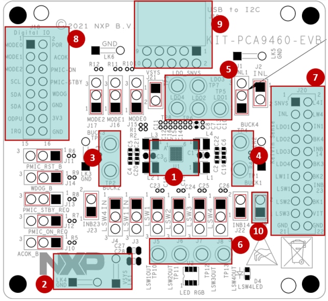
- PCA9460 PIMC
- VSYS and GND main input power connectors
- Buck 2 and Buck 3 output test points
- Buck 1 and Buck 4 output test points
- LDO output test points
- Load switch output test points
- Kevin sense connector
- USB to I2C connector
- I2C pull-up voltage jumper (OD_PU)
3. Get Software
3.1 Install Software
Installing software is necessary to work with this evaluation board
- Go to KIT-PCA9460-EVB
- Extract the zip file PCA9460_EVB_GUI_1.20.08.18.zip Evaluation Kit GUI file into selected folder. No need to install (if password is asked during unzip, then type “NXP”)
- Install the FTDI cable driver from website Drivers
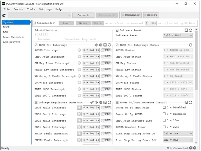
- Run the file PCA9460.exe. The interface window is shown in Figure 2
4. Configure Hardware
4.1 Configure the Hardware for Startup
Connect the wires of the FTDI cable on the following pins and make sure the power supply is turned Off and the USB connector is disconnected during the wiring stage:

-
Connect both SDA, the SCL, the GND, and the 3.3 V wires from the FTDI cable.
- a. SCL serial clock signal (orange cable) should be connected to pin 7 of the 'Digital IO' connector (
J18) - b. Both SDA serial data wires (yellow and green cables) should be connected to create bidirectional data. Connect yellow cable to pin 9, and green cable to pin 11 of the 'Digital IO' connector (
J18) - c. GND ground signal (black cable) should be connected to pin 12 or pin 16 of the 'Digital IO' connector (
J18) - d. 3.3 V supply wire (red cable) should be connected to pin 14 of the 'Digital IO' connector (
J18)
- a. SCL serial clock signal (orange cable) should be connected to pin 7 of the 'Digital IO' connector (
- With the power supply turned Off, connect 5.0 V power supply to LK1 connector and corresponding ground to LK4
- Turn On power supply.
- Connect USB connector of the FDTI cable to PC
Design Resources
Additional References
In addition to our PCA9460: 13-Channel Power Management Integrated Circuit (PMIC) for Ultra Low Power Application page, you may also want to visit:
- i.MX7ULP: i.MX 7ULP Family, Ultra-Low-Power with Graphics
- i.MX 8ULP Applications Processor Family
- PCA9420: PMIC for Low Power Applications
Application pages:
- Smart Watch and Wristband
- Transport ticketing
- Building Security and Surveillance
- Robotic appliances
- Small and medium appliances