Design Files
Receive the full breakdown. See the product footprint and more in the eCad file.
Building on the successful Kinetis K Series (K22 and K24), the K32 L3 family of MCUs delivers a 50% improvement in power optimization and security advancements over the previous generation, to address a wide range of industrial and IoT applications. The K32 L3 MCU family is based on the power-efficient Arm® Cortex® -M4 core and offers a Cortex-M0+, providing new enhancements such as low-leakage power-optimized peripherals, a DC-DC converter, and security features like authenticated boot, secure update and tamper detection pins.
The introduction of the K32 L3 MCU family is the start of a long line of MCUs, which will further advance NXP's security capabilities and power optimization features to lead the market in the next generation of low-leakage applications. The K32 L3 MCU family is complemented by a comprehensive ecosystem including MCUXpresso software and tools and a Freedom development board for easy prototyping.
|
|
|
|
|
|
|
|---|---|---|---|---|---|
|
|
|
|
|
|
|
|
|
|
|
|
|
|
|
|
|
|
|
|
|
|
|
|
|
|
|
|
|
|
|
|
|
|
|
|
|
|
|
|
|
|
|
|
|
|
|
|
|
|
|
|
|
|
|
|
|
|
|
|
|
|
|
|
|
|
|
|
|
|
Quick reference to our documentation types.
5 documents
Please wait while your secure files are loading.
Receive the full breakdown. See the product footprint and more in the eCad file.

Receive the full breakdown. See the product footprint and more in the eCad file.
1-5 of 9 hardware offerings
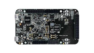

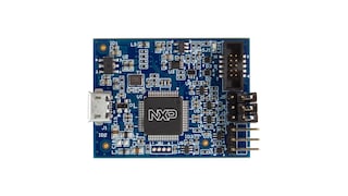
Additional hardware available. View our featured partner solutions.

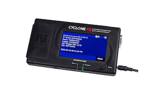
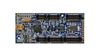
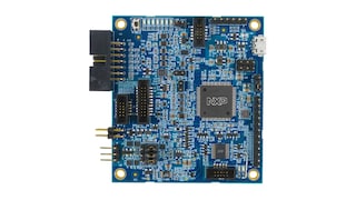

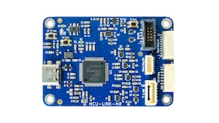
2 hardware offerings


To find additional partner offerings that support this product, visit our Partner Marketplace.
Quick reference to our software types.
5 software files
Additional software available. View our featured partner solutions.
Note: For better experience, software downloads are recommended on desktop.
Please wait while your secure files are loading.
1-5 of 7 software offerings


To find additional partner offerings that support this product, visit our Partner Marketplace.
1-5 of 8 engineering services


There are no results for this selection.
To find additional partner offerings that support this product, visit our Partner Marketplace.
1 trainings
4 trainings
To find additional partner offerings that support this product, visit our Partner Marketplace.