

Receive the full breakdown. See the product footprint and more in the eCad file.
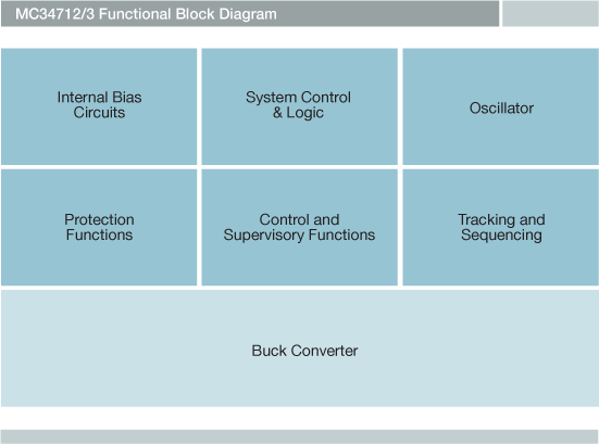
The NXP® MC34712 is a highly-integrated, space-efficient, low-cost, single-synchronous buck switching regulator with integrated N-channel power MOSFETs.
Quick reference to our documentation types.
5 documents
Compact List
5 documents
Compact List
Receive the full breakdown. See the product footprint and more in the eCad file.
There are no recently viewed products to display.