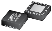
Multiplexer / Demultiplexer Switch for Thunderbolt Applications

  • This page contains information on a product that is no longer manufactured (discontinued). Specifications and information herein are available for historical reference only.

See product image

Product Details

Block Diagram

CBTL05023 Block Diagram

CBTL05023 Block Diagram

Features

AUX MUX 2: 1 Switch

  • This 2 : 1 switch is controlled by CA_DET signal multiplexing of the 1 Mbit/s differential AUX and DDC (Direct Display Control) signals
    • When CA_DET is HIGH, DDC path is selected
  • Differential AUX channel:
    • Low insertion loss: -0.5 dB at 5 MHz
    • Low return loss: -19 dB at 5 MHz
    • Low ON-state resistance: 7.5 Ω
    • Bandwidth: 5 GHz
    • Low off-state isolation: -75 dB at 5 MHz
    • Low crosstalk: -40 dB at 5 MHz
    • Common-mode input voltage VIC: 0 V to 3.3 V
    • Differential input voltage VID: 1.4 V (maximum)
  • DDC channel has DDC_CLK and DDC_DAT IC²C signals
    • 100 kHz 3.3 V voltage swing
  • Both AUXIO+ and AUXIO- outputs have 900 Ω (±20 %) pull-down resistor that is enabled by the status of the BIASOUT output pin
    • These pull-down resistors provide DC bias for the 10 Gbit/s channel

DP MUX 2: 1 Switch

  • The DP MUX is a 2: 1 switch that is controlled by DP_PD pin multiplexing of a differential DPML signal and LSTX/LSRX signals
  • The DPML (DisplayPort Main Link) runs up to HBR2 data rate of 5.4 Gbit/s
  • The low speed DC coupled signals LSTX and LSRX are 3.3 V single-ended signals that operated at 1 Mbit/s
  • 5.4 Gbit/s DPML channel:
    • Low insertion loss for DP-DPMLO path: -2.0 dB at 2.5 GHz
    • Low insertion loss for LS-DPMLO path: -2.0 dB at 2.5 GHz
    • Low return loss for DP-DPMLO path: -15 dB at 2.5 GHz
    • Low return loss for LS-DPMLO path: -14 dB at 2.5 GHz
    • Low ON-state resistance for DP-DPMLO path: 9 Ω
    • Low ON-state resistance for LS-DPMLO path: 13 Ω
    • High bandwidth: 7 GHz
    • Low off-state isolation: -20 dB at 2.5 GHz
    • Low crosstalk: -25 dB at 2.5 GHz
    • Common-mode input voltage VIC: 0 V to 3.3 V
    • Differential input voltage VID: 1.4 V (maximum)

General

  • The input of the HPDOUT (Hot Plug Detect output) buffer is 5 V tolerant
  • HPDOUT, CA_DETOUT and BIASOUT buffers
    • CA_DET input leakage current < 0.1 μA to prevent driving the 1 MΩ pull-down to a HIGH level
    • BIASOUT buffer is able to provide enough current to drive the bias circuit for the PIN diode path
    • BIASOUT buffer can drive up to six sets of bias circuits for the 10 Gbit/s paths
  • When AUXIO_EN is LOW or (BIASIN = 0 and DP_PD = 1), this chip is in Sleep mode
    • AUXIO+ and AUXIO- of AUX MUX are disabled
    • CA_DETOUT and HPDOUT buffers are on
    • When the chip is in Sleep mode, CBTL05023 will consume < 3.5 mW
  • High-bandwidth analog pass-gate technology
  • Very low intra-pair differential skew (5 ps typical)
  • All channels have back current protection
  • All channels support rail-to-rail input voltage
  • CMOS input buffer with hysteresis
  • Single 3.3 V ± 10 % power supply
  • HVQFN24 3 mm x 3 mm package, 0.4 mm pitch, with exposed center pad for thermal relief and electrical ground
  • ESD: 2500 V HBM, 1250 V CDM
  • Operating temperature range: 0 °C to 85 °C

Documentation

Quick reference to our documentation types.

3 documents

Design Files

Support

What do you need help with?