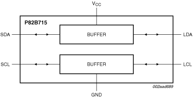
The P82B715 is a bipolar IC intended for application in IC-bus and derivative bus systems. While retaining all the operating modes and features of the IC-bus it permits extension of the practical separation distance between components on the I²C-bus by buffering both the data (SDA) and the clock (SCL) lines.
The IC-bus capacitance limit of 400 pF restricts practical communication distances to a few meters. Using one P82B715 at each end of a long cable (connecting Lx/Ly to Lx/Ly) reduces that cables loading on the linked IC-buses by a factor of 10 and allows the total system capacitance load (all devices, cable, connectors, and traces or wires connected to the IC-bus) to be around 3000 pF while the loading on each IC-bus on the Sx/Sy sides remains below 400 pF. Longer cables or low-cost, general-purpose wiring may be used to link IC-bus based modules without degrading noise margins. Multiple P82B715s can be connected together, linking their Lx/Ly ports, in a star or multi-point architecture as long as the total capacitance of the system is less than about 3000 pF and each bus at an Sx/Sy connection is well below 400 pF. This configuration, with the controller and/or devices attached to the Sx/Sy port of each P82B715, has full multi-controller communication capability. The P82B715 alone does not support voltage level translation, but it can be simply implemented using low cost transistors when required. There is no restriction on interconnecting the Sx/Sy I/Os, and, because the device output levels are always held within 100 mV of input drive levels, P82B715 is compatible with bus buffers that use voltage level offsets, e.g., PCA9511A, PCA9517, Sx/Sy side of P82B96.
The lower VOL level and ability to operate with any controller, target or bus buffer is the primary advantage of the using the P82B715 for long distance buses at the disadvantage of not isolating bus capacitance like the P82B96 or PCA9600 are able to do. The primary disadvantage of the P82B96 and PCA9600 is that the static level offset needed to isolate bus capacitance does not allow these devices to operate with other bus buffers with special offset levels or with controller/target that require a VIL lower than 0.8 V with noise margin. A proven quick design-in point-to-point/multi-point circuit is included in Section 8.2 to allow rapid use of the P82B715 along with comparison waveforms so that the designer can clearly see the trade-offs between the P82B715 and the P82B96/PCA9600 and choose the type of device that is best for their application.


