Application Note (2)
-
PicoGate Logic footprints[AN10161]
Data Sheet (1)
Package Information (2)
Packing Information (2)
Supporting Information (1)
-
MAR_SOT833 Topmark[MAR_SOT833]
Sign in for a personalized NXP experience.
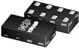
The NX3L2G66 is a dual low-ohmic single-pole single-throw analog switch. Each switch has two input/output terminals (nY and nZ) and an active HIGH enable input (nE). When pin nE is LOW, the analog switch is turned off.
Schmitt trigger action at the enable input (nE) makes the circuit tolerant to slower input rise and fall times. The NX3L2G66 allows signals with amplitude up to VCC to be transmitted from nY to nZ; or from nZ to nY. Its low ON resistance (0.5 Ω) and flatness (0.13 Ω) ensures minimal attenuation and distortion of transmitted signals.

1 result
Exclude 1 NRND
Part | CAD Model | Family | Status | Configuration | Function | VCC (V) | Logic switching levels | RON (Ohm) | RON(FLAT) | f(-3dB) (MHz) | THD (%) | Xtalk (dB) | Power dissipation considerations | Tamb (°C) | Rth(j-a) (K/W) | th(j-top) (K/W) | Package Type | Number of pins |
|---|---|---|---|---|---|---|---|---|---|---|---|---|---|---|---|---|---|---|
NX3 | No Longer Manufactured | SPST-NO | dual single-pole, single-throw analog switch | 1.4 - 4.3 | CMOS/LVTTL | 0.75 | 0.3 | 60 | 0.0024 | -90 | ultra low | -40~125 | 251 | 128 | XSON8 | 8 |
Quick reference to our documentation types.
8 documents
Compact List
There are no results for this selection.
Please wait while your secure files are loading.
8 documents
Compact List
1 design file
Please wait while your secure files are loading.
1 design file
There are no recently viewed products to display.

Help us improve your experience on our site. We invite you to take our five-question survey.