Most power semiconductor devices are constructed in a very similar way. The active part of the device, or ‘die’, is soldered to some form of copper tab or leadframe. Pins or legs are added to make connections to the PCB and the whole thing is either partially or completely encapsulated in plastic. Alternatively for most surface-mount devices, the outer surface of the tab is exposed so that the device may be soldered to a PCB, with the tab also providing the thermal and electrical pathway from the die to the outside world. This is the method of construction employed in D2PAK and DPAK devices for instance, which you may be familiar with.
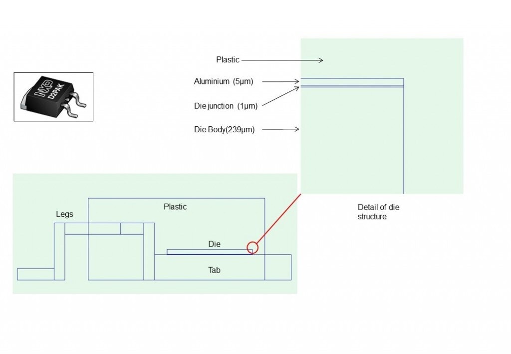
The thermal simulation model of a typical NXP D2PAK device is shown in Fig. 1. This is an example of a ‘detailed’ thermal model, which, as the name suggests, includes discretely modeled elements such as the die, legs and tab.

Fig. 1 An NXP D2PAK MOSFET (top left), its detailed thermal model (bottom left) and detail of the die structure (right)
For an NXP power MOSFET the die model is more refined than just a simple slab of silicon with uniform power dissipation. As you can see from Fig.1, the die has an overall thickness of 240 µm. This is split into two parts: the Die Body, which is thermally conductive but non-dissipative, and the thinner Die Junction which is thermally conductive and the source of the die dissipation when the device is conducting current. And on top of the die we have a 5 µm layer of aluminum. This level of die detail is essential when carrying out device transient thermal analyses.
Because of the non-uniform nature of the die, it is not immediately obvious how the heat energy will flow through the device when the Die Junction is dissipating or how the temperature in the various parts of the device will rise over time. Using simulations, we can model these effects very easily, as I will now demonstrate.
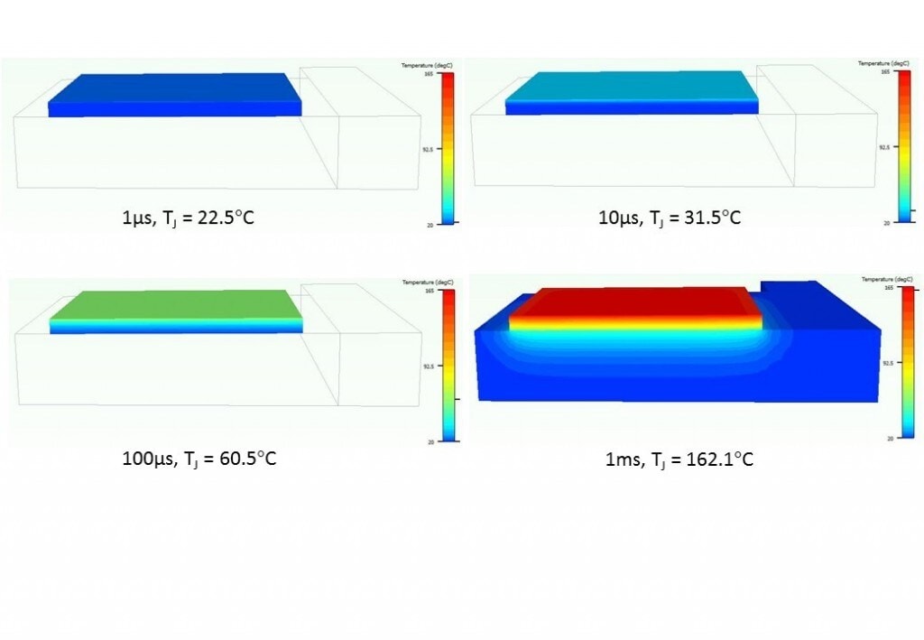
For the purposes of this exercise we will use a simulation model of a D2PAK MOSFET mounted on a PCB. Using the detailed device model shown in Fig. 1 we will run several transient thermal simulations of different durations and observe the temperature rise and heat flow in the die. Starting temperature is 20 °C in all cases and the simulation durations (or power pulse widths) will be 1 µs, 10 µs, 100 µs and 1 ms. In all cases power dissipation in the Die Junction is 1500 W and junction temperature TJ is recorded at the center of the Die Junction. Temperature plots from the simulation are shown in Fig. 2. To aid clarity I have taken a slice through the center of the model, hidden the plastic and the legs and made the tab transparent in three cases. I have done this to make the development of temperature within the device die more clearly visible.

Fig. 2 Temperature plots for the D2PAK MOSFET after 1 µs, 10 µs, 100 µs and 1 ms.
Some interesting observations:
- After 1 µs – TJ has hardly increased at all. Even though the Die Junction power dissipation could be considered high (1500 W), the total energy dissipated in the device is still only 1.5 mW.
- After 100 µs – approximately half the thickness of the die is still at the starting temperature and TJ is a relatively modest 60.5 °
- At 1ms – we finally see heat energy beginning to spread into the top of the tab and TJ is approaching the maximum limit for the device of 175 °
If we were to look at the heat flow through the various parts of the structure we would find that, after 1ms, less than 1% of the total heat energy is leaving the device through the bottom of the tab, and even less than that through the plastic surrounding the device. This leads us to perhaps the most interesting and useful conclusion of all.
- For single power pulses of duration up to 1 ms, even with a large amplitude, the majority of the heat transfer and temperature change occurs within the confines of the device. Any attached PCB or heat sink is irrelevant in this timeframe.
Additional exercises carried out for other power packages (DPAK, TO220, LFPAK, etc.) have resulted in similar conclusions.
In the next post I’ll look at how we can modify the temperature development within the device using a top clip to provide thermal advantages under certain conditions.


