Application Note (5)
Data Sheet (1)
Errata (1)
-
Errata sheet LPC43S50, LPC43S30, LPC43S20[ES_LPC43SX0]
Fact Sheet (1)
-
LPC43Sxx Series of MCUs - Fact Sheet[LPC43SXXLF]
Sign in for a personalized NXP experience.
The LPC43S70FET256 is a Arm Cortex-M4 based microcontroller for embedded applications which includes an Arm Cortex-M0 coprocessor and an Arm Cortex-M0 subsystem for managing peripherals, 282 kB of SRAM, advanced configurable peripherals such as the State Configurable Timer (SCTimer/PWM) and the Serial General Purpose I/O (SGPIO) interface, security features with AES engine, two High-speed USB controllers, Ethernet, LCD, an external memory controller, and multiple digital and analog peripherals including a high-speed 12-bit ADC. The LPC43S70FET256 operates at CPU frequencies of up to 204 MHz.
The Arm Cortex-M4 is a 32-bit core that offers system enhancements such as low power consumption, enhanced debug features, and a high level of support block integration. The Arm Cortex-M4 CPU incorporates a 3-stage pipeline, uses a Harvard architecture with separate local instruction and data buses as well as a third bus for peripherals, and includes an internal prefetch unit that supports speculative branching. The Arm Cortex-M4 supports single-cycle digital signal processing and SIMD instructions. A hardware floating-point unit is integrated in the core. The Arm Cortex-M4 with floating-point unit is often referred to as M4F.
The LPC43S70 include an application Arm Cortex-M0 coprocessor and a second Arm Cortex-M0 subsystem for managing the SGPIO and SPI peripherals. The Arm Cortex-M0 core is an energy-efficient and easy-to-use 32-bit core which is code- and tool-compatible with the Cortex-M4 core. Both Cortex-M0 cores offer up to 204 MHz performance with a simple instruction set and reduced code size. The Cortex-M0 does not support hardware multiply.

| | | | | |
|---|---|---|---|---|---|
| | | | | |
| | | | | |
| | | | | |
| | | | | |
| | | | | |
| | | | | |
| | | | | |
| | | | | |
| | | | | |
| | | | | |
LPC43S70FET256Quick reference to our documentation types.
1-10 of 12 documents
Compact List
There are no results for this selection.
Sign in to access authorized secure files. Learn more about secure access rights.
Please wait while your secure files are loading.
1-10 of 12 documents
Compact List
2 design files
Sign in to access authorized secure files. Learn more about secure access rights.
Please wait while your secure files are loading.
2 design files
1-5 of 8 hardware offerings
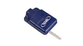
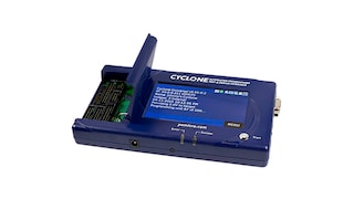
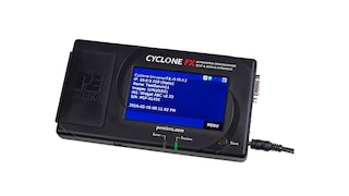
Additional hardware available. View our featured partner solutions.
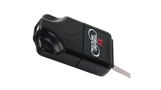
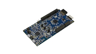
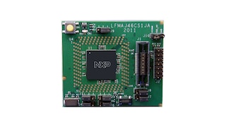
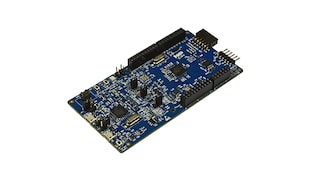

Sign in to access authorized secure files. Learn more about secure access rights.
1 hardware offering
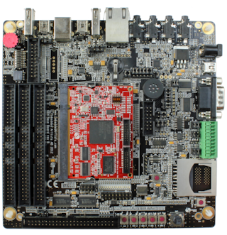
To find additional partner offerings that support this product, visit our Partner Marketplace.
1-5 of 8 hardware offerings


Additional hardware available. View our featured partner solutions.


Quick reference to our software types.
5 software files
Additional software available. View our featured partner solutions.
Note: For better experience, software downloads are recommended on desktop.
Sign in to access authorized secure files. Learn more about secure access rights.
Please wait while your secure files are loading.
1-5 of 34 software offerings
To find additional partner offerings that support this product, visit our Partner Marketplace.
5 software files
Additional software available. View our featured partner solutions.
Note: For better experience, software downloads are recommended on desktop.
1-5 of 7 engineering services


There are no results for this selection.
There are no results for this selection.
To find additional partner offerings that support this product, visit our Partner Marketplace.
1-5 of 10 trainings
To find additional partner offerings that support this product, visit our Partner Marketplace.
1-5 of 10 trainings
To find additional partner offerings that support this product, visit our Partner Marketplace.

Help us improve your experience on our site. We invite you to take our five-question survey.