Design Files
1 design file
Receive the full breakdown. See the product footprint and more in the eCad file.
-
Models
BSDL for LPC313x and LPC314x pkg TFBGA
The NXP LPC3141 combine a 270 MHz ARM926EJ-S CPU core, High-speed USB 2.0 OTG, 192 kB SRAM, NAND flash controller, flexible external bus interface, four channel 10-bit A/D, and a myriad of serial and parallel interfaces in a single chip targeted at consumer, industrial, medical, and communication markets. To optimize system power consumption, the LPC3141 have multiple power domains and a very flexible Clock
Part numbers include: LPC3141FET180.
|
|
|
|
|
|
---|---|---|---|---|---|
|
|
|
|
|
|
|
|
|
|
|
|
|
|
|
|
|
|
|
|
|
|
|
|
|
|
|
|
|
|
|
|
|
|
|
|
|
|
|
|
|
|
|
|
|
|
|
|
|
|
|
|
|
|
|
|
|
|
|
|
Quick reference to our documentation types.
1-5 of 7 documents
Please wait while your secure files are loading.
1 design file
Receive the full breakdown. See the product footprint and more in the eCad file.
Please wait while your secure files are loading.
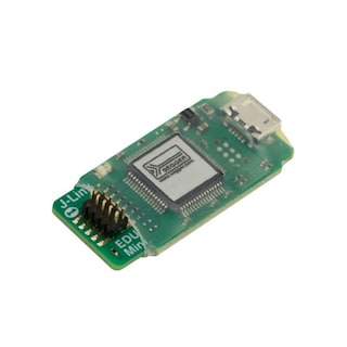
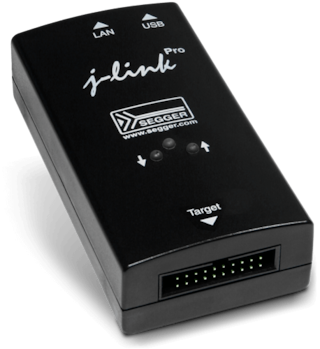
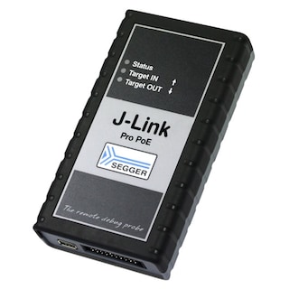
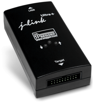
3 hardware offerings
To find additional partner offerings that support this product, visit our Partner Marketplace.
Quick reference to our software types.
1-5 of 12 software offerings
Please wait while your secure files are loading.
1-5 of 12 software offerings
To find additional partner offerings that support this product, visit our Partner Marketplace.
1-5 of 7 engineering services
There are no results for this selection.
To find additional partner offerings that support this product, visit our Partner Marketplace.
4 trainings
4 trainings
To find additional partner offerings that support this product, visit our Partner Marketplace.