Design Files
2 design files
-
Models
IBIS models for LPC29xx
-
Symbols and Footprints
LPC2xxx ORCAD symbols
Sign in for a personalized NXP experience.
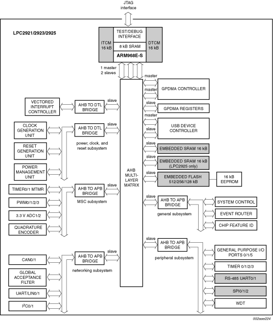
The LPC2921/2923/2925 combine an ARM968E-S CPU core with two integrated TCM blocks operating at frequencies of up to 125 MHz, Full-speed USB 2.0 device controller, CAN and LIN, up to 40 kB SRAM, up to 512 kB flash memory, two 10-bit ADCs, and multiple serial and parallel interfaces in a single chip targeted at consumer, industrial, and communication markets. To optimize system power consumption, the LPC2921/2923/2925 has a very flexible Clock Generation Unit (CGU) that provides dynamic clock gating and scaling.
1 result
Exclude 1 NRND
Part | Order | CAD Model | SCTimer / PWM | Package Type | Temperature range | Status | Product category |
---|---|---|---|---|---|---|---|
1 | LQFP100 | -40 °C to +85 °C | End of Life | 160-LPC2900- |
Quick reference to our documentation types.
1-5 of 13 documents
There are no results for this selection.
Please wait while your secure files are loading.
1-5 of 13 documents
2 design files
Please wait while your secure files are loading.
2 design files