Data Sheet (1)
Package Information (1)
Supporting Information (1)
-
Brief CBTV24DD12[BRIEF_CBTV24DD12]
Sign in for a personalized NXP experience.
The CBTV24DD12 is designed for 1.8 V / 2.5 V / 3.3 V supply voltage operation and it supports Pseudo Open Drain (POD), SSTL_12, SSTL_15 or SSTL_18 signaling and CMOS select input levels. This device is designed for operation in DDR4, DDR3 or DDR2 memory bus systems, with speeds up to 3200 MT/s.
The CBTV24DD12 has a 1:2 switch or 2:1 multiplex topology and offers a 12-bit wide bus. Each 12-bit wide A-port can be switched to one of two ports B and C, for all bits simultaneously. Each port is non-directional due to the use of FET switches, allowing a multitude of applications requiring high-bandwidth switching or multiplexing.
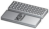
The selection of the port is by a simple CMOS input (SELect). Another CMOS input (ENable) is available to allow all ports to be disconnected. The SEL0, SEL1 and EN input signals are designed to operate transparently as CMOS input level signals up to 3.3 V. The CBTV24DD12 uses NXP’s proprietary high-speed switch architecture providing high bandwidth, very little insertion loss, return loss, and very low propagation delay, allowing use in many applications requiring switching or multiplexing of high-speed signals. It is available in a 3.0 mm x 8.0 mm TFBGA48 package with 0.65 mm ball pitch, for optimal size versus board layout density considerations. It is characterized for operation from -10 °C to +85 °C.

Quick reference to our documentation types.
3 documents
Compact List
There are no results for this selection.
Sign in to access authorized secure files. Learn more about secure access rights.
Please wait while your secure files are loading.
3 documents
Compact List
There are no recently viewed products to display.

Help us improve your experience on our site. We invite you to take our five-question survey.