
Product Longevity
Participating products are available for a minimum of 10 years. Designated participating products developed for the automotive, telecom and medical segments are available for a minimum of 15 years.
Sign in for a personalized NXP experience.
Designed for body electronics, the NXP MPC5510 MCU belongs to an expanding family of automotive-focused products that address the next wave of central body and gateway applications within the vehicle.

Participating products are available for a minimum of 10 years. Designated participating products developed for the automotive, telecom and medical segments are available for a minimum of 15 years.
| | | | | |
|---|---|---|---|---|---|
| | | | | |
| | | | | |
| | | | | |
| | | | | |
| | | | | |
| | | | | |
| | | | | |
| | | | | |
| | | | | |
| | | | | |
Quick reference to our documentation types.
1-10 of 52 documents
Compact List
There are no results for this selection.
Sign in to access authorized secure files. Learn more about secure access rights.
Please wait while your secure files are loading.
1-10 of 52 documents
Compact List
2 design files
Sign in to access authorized secure files. Learn more about secure access rights.
Please wait while your secure files are loading.
2 design files
1-5 of 7 hardware offerings
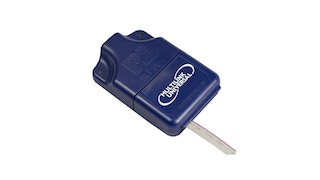
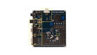
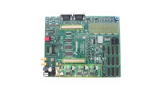
Additional hardware available. View our featured partner solutions.
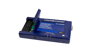
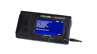
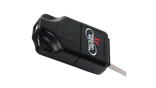
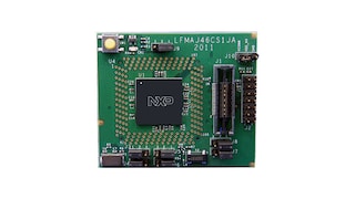
Sign in to access authorized secure files. Learn more about secure access rights.
3 hardware offerings
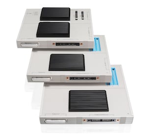
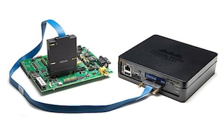
To find additional partner offerings that support this product, visit our Partner Marketplace.
1-5 of 7 hardware offerings


Additional hardware available. View our featured partner solutions.


Quick reference to our software types.
4 software files
Additional software available. View our featured partner solutions.
Note: For better experience, software downloads are recommended on desktop.
Sign in to access authorized secure files. Learn more about secure access rights.
Please wait while your secure files are loading.
1-5 of 10 software offerings
To find additional partner offerings that support this product, visit our Partner Marketplace.
4 software files
Additional software available. View our featured partner solutions.
Note: For better experience, software downloads are recommended on desktop.
1-5 of 13 engineering services


.svg)


There are no results for this selection.
There are no results for this selection.
To find additional partner offerings that support this product, visit our Partner Marketplace.
5 trainings
To find additional partner offerings that support this product, visit our Partner Marketplace.
5 trainings
To find additional partner offerings that support this product, visit our Partner Marketplace.
There are no recently viewed products to display.

Help us improve your experience on our site. We invite you to take our five-question survey.